Using energy harvesting implementations in aircraft design(2)
Energy harvesting basics
Transducers that create electricity from readily available physical sources such as temperature differentials (thermoelectric generators or thermopiles), mechanical vibration or strain (piezoelectric or electromechanical devices) and light (photovoltaic devices) are viable sources of power for many applications. Numerous wireless sensors, remote monitors, and other low-power applications are on track to become near “zero” power devices using only harvested energy.
Even though the concept of energy harvesting has been around for a number of years, the implementation of a system in a real world environment has been cumbersome, complex and costly. Nevertheless, examples of markets where an energy harvesting approach has been used include transportation infrastructure, wireless medical devices, tire pressure sensing, and building automation.
A typical energy scavenging configuration or system (represented by the four main circuit system blocks shown in figure 1), usually consists of a free energy source. Examples of such sources include a thermoelectric generator (TEG) or thermopile attached to a heat-generating source such as an aircraft engine, or a piezoelectric transducer attached to a vibrating mechanical source such as an aircraft airframe or wing. In the case of a heat source, a compact thermoelectric device can convert small temperature differences into electrical energy. And where vibration or strain is available, a piezoelectric device can convert these small vibrations or strain differences into electrical energy. In either case, the electrical energy produced can be converted by an energy harvesting circuit (the second block in Figure 1) and modified into a usable form to power downstream circuits. These downstream electronics usually consist of some kind of sensor, an analog-to-digital converter and an ultralow power microcontroller (the third block in figure 1). These components can take this harvested energy, now in the form of an electric current, and wake up a sensor to take a reading or a measurement and then make this data available for transmission via an ultralow power wireless transceiver – represented by the fourth block in the circuit chain shown in figure 1. Figure 1: The four main blocks of a typical energy-scavenging system.
Using energy harvesting implementations in aircraft design
ENERGY HARVESTING
Each circuit system block in this chain, with the possible exception of the energy source itself, has had its own unique set of constraints that have impaired its economical viability until now.
Low cost and low power sensors and microcontrollers have been available for a couple of years; however, it is only recently that ultralow power transceivers have become commercially available. Nevertheless, the laggard in this chain has been the energy harvester. Existing implementations of the energy harvester block typically consist of low performing discrete configurations, usually comprising 30 or more components. Such designs have low conversion efficiency and high quiescent currents. Both of these deficiencies result in compromised performance in end-systems. The low conversion efficiency increases the amount of time required to power up a system, which in turn increases the time interval between taking a sensor reading and transmitting the data. A high quiescent current limits how low the output of the energy-harvesting source can be, since it must first overcome the current level needed for its own operation before it can supply any excess power to the output.
Transducers and ICs The core component of a thermoelectric device is a thermocouple, which consists of an ntype and a p-type semiconductor connected by a metal plate. Electrical connection at the opposing ends of the p- and n-type material complete an electric circuit. Thermoelectric generation (TEG) occurs when the couple is subjected to a thermal gradient, in which case the device generates a voltage and causes current to flow, thereby converting heat into electrical power by what is known as the Seebeck effect. A thermoelectric module is then formed from arrays of these thermocouples connected in series.
If heat is flowing between the top and bottom of the module, a voltage will be produced and an electric current will flow. In the case of a typical airplane engine, its temperature can vary anywhere from a few 100oC to 1,000 to 2,000oC. Although most of this energy is lost in the form of mechanical energy (from combustion and thrust), a portion is dissipated purely as heat. Since the Seebeck effect is the underlying thermodynamic phenomenon that converts thermal heat to electric power, the main equation to take into consideration is: P = ηQ where P is electrical power, Q is heat and η is efficiency. Larger TEGs that use more heat, Q, produce more power, P. Similarly, the use of twice as many power converters naturally produces twice the power, given that they can capture twice the heat. Larger TEGs are created by putting more P-N junctions in series; however, while this creates more millivolts per delta T (mV/dT), it also increases the series resistance of the TEG. This increased series resistance limits the power available to the load. Therefore, depending on the application requirements, it is sometimes better to use smaller TEGs in parallel rather than using a larger TEG. Regardless of which choice is used, TEGs are commercially available from a number of suppliers, including Tellurex Corp. Piezoelectricity can be generated by applying stress to an element, which in turn creates an electric potential. The piezoelectric effect is reversible in that materials exhibiting the direct piezoelectric effect (the production of an electric potential when stress is applied) also exhibit the reverse piezoelectric effect (the production of stress and/or strain when an electric field is applied). In order to optimize a piezo transducer, one needs to characterize their source for vibration frequency and displacement. Once these levels have been determined, a piezo manufacturer can design a piezo that is mechanically tuned to the specific vibration frequency and size it to provide the necessary amount of power. The vibration in the Piezo material activates the Direct Piezo effect, which results in the accumulation of charge on the output capacitance of the device. This is usually pretty small so the AC open circuit voltage is high—on the order of 200 Volts in many cases. Since the amount of charge generated from each deflection is relatively small, it is necessary to full-wave rectify this AC signal and accumulate the cycle-by-cycle charge on an input capacitor. Once again, there are a number of piezoelectric transducers commercially available from a number of suppliers, including AmbioSystems, MIDE Technology Corp. and Advanced Cerametrics Inc.
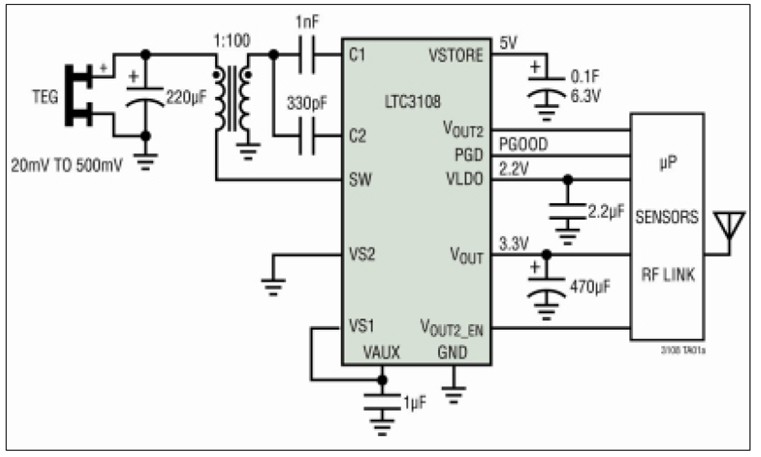
However, what has been missing until now has been a highly integrated, high efficiency DC/ DC converter solution that can both harvest and manage the energy from either a thermal or piezoelectric source. The LTC3108 is a voltage stepup converter and power manager specifically designed to greatly simplify the task of harvesting and managing surplus energy from extremely low input voltage sources such as thermopiles, TEGs and even small solar panels. Its step-up topology operates from input voltages as low as 20mV. This allows the LTC3108 to harvest energy from a TEG with as little as 1°C temperature differential. The circuit shown in figure 2 uses a small step-up transformer to boost the input voltage source to a LTC3108 which then provides a complete power management solution for wireless sensing and data acquisition. It can harvest small temperature differences and generate system power instead of using traditional battery power.
LTC3108
The LTC3108 utilizes a depletion mode N-channel MOSFET switch to form a resonant step-up oscillator using an external step-up transformer and a small coupling capacitor. This allows it to boost input voltages as low as 20mV, high enough to provide multiple regulated output voltages for powering other circuits. The frequency of oscillation is determined primarily by the inductance of the transformer’s secondary winding and input capacitance of the LTC3108 and is typically in the range of 20kHz to 200kHz. For input voltages as low as 20mV, a primary-secondary turns ratio of about 1:100 is recommended. For higher input voltages, a lower turns ratio can be used, since it will provide greater output power. These transformers are standard, off-the-shelf components, and are readily available from magnetic suppliers. Linear’s compound depletion mode N-channel MOSFET is what makes 20mV operation possible.
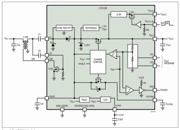
As can be seen in figure 3, the LTC3108 takes a “systems level” approach to solving a complex problem. It can convert the low voltage source and manage the energy between multiple outputs. The AC voltage produced on the secondary winding of the transformer is boosted and rectified using an external charge pump capacitor (from the secondary winding to pin C1) and the rectifiers internal to the LTC3108. This rectifier circuit feeds current into the VAUX pin, providing charge to the external VAUX capacitor and then the other outputs. The internal 2.2V LDO can support a low-power processor or other low power ICs. The LDO is powered by the higher value of either VAUX or VOUT. This enables it to become active as soon as VAUX has charged to 2.3V, while the VOUT storage capacitor is still charging. In the event of a step load on the LDO output, current can come from the main VOUT capacitor if VAUX drops below VOUT. The LDO output can supply up to 3mA.
LTC3588-1 The main output voltage on VOUT is charged from the VAUX supply and is user programmable to one of four regulated voltages using the voltage select pins VS1 and VS2. The four fixed output voltages are: 2.35V for supercapacitors, 3.3V for standard capacitors and RF or sensor circuitry, 4.1V for lithium-ion battery termination or 5V for higher energy storage and a main system rail to power a wireless transmitter or sensors – thereby eliminating the need for multi-meg-Ohm external resistors. As a result, the LTC3108 does not require special board coatings to minimize leakage, as do discrete designs where very large value resistors are required. A second output, VOUT2, can be turned on and off by the host microprocessor using the VOUT2_ EN pin. When enabled, VOUT2 is connected to Vout through a P-channel MOSFET switch. This output can be used to power external circuits such as sensors or amplifiers that do not have low power sleep or shutdown capability. An example of this would be to power a MOSFET on and off as part of a sensing circuit within a building thermostat. The VSTORE capacitor may be a very large value (thousands of microfarads or even farads), to provide holdup at times when the input power may be lost. Once power-up is completed, the main, backup and switched outputs are all available.
If the input power fails, operation can still continue, operating off the VSTORE capacitor. The VSTORE output can be used to Figure 3: The LTC3108 block diagram. charge a large storage capacitor or rechargeable battery after VOUT has reached regulation. Once VOUT has reached regulation, the VSTORE output is allowed to charge up to the VAUX voltage, which is clamped at 5.3V. Not only can the storage element on VSTORE be used to power the system if the input source is lost, but it can also be used to supplement the current demanded by VOUT, VOUT2 and the LDO outputs if the input source has insufficient energy.
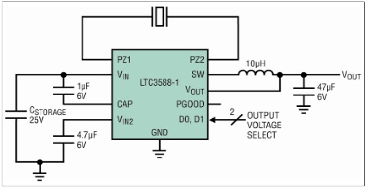
A power good comparator monitors the VOUT voltage. Once VOUT has charged to within 7 percent of its regulated voltage, the PGOOD output will go high. If VOUT drops more than 9 percent from its regulated voltage, PGOOD will go low. The PGOOD output is designed to drive a microprocessor or other chip I/O and is not intended to drive a higher current load such as a LED. The circuit shown in figure 4 utilizes a small piezoelectric transducer to convert mechanical vibration into an AC voltage source that is fed into the LTC3588-1’s internal bridge rectifier. It can harvest energy from small vibration sources and generate system power instead of using traditional battery power.
The LTC3588-1 is a quiescent current power supply designed specifically for energy harvesting and/or low current step-down applications. It can interface directly to a piezoelectric or alternative AC power source, rectify the voltage waveform and store harvested energy in an external capacitor, bleed off any excess power via an internal shunt regulator and maintain a regulated output voltage by means of a nanopower buck regulator. The LTC3588-1’s internal fullwave bridge rectifier is accessible via two differential inputs, PZ1 and PZ2, which rectify AC inputs. This rectified output is then stored on a capacitor at the VIN pin and can be used as an energy reservoir for the buck converter. The low-loss bridge rectifier has a total voltage drop of about 400mV with typical piezo generated currents, which are normally around 10μA. This bridge is capable of carrying up to 50mA of current. The buck regulator is enabled once there is sufficient voltage on VIN to produce a regulated output. The buck regulator uses a hysteretic voltage algorithm to control the output through internal feedback from the VOUT sense pin. The buck converter charges an output capacitor through an inductor to a value slightly higher than the regulation point. It does this by ramping the inductor current to 260mA through an internal PMOS switch and then ramping it down to 0mA through an internal NMOS switch, thereby efficiently delivering energy to the output capacitor. Its hysteretic method of providing a regulated output reduces losses associated with FET switching and maintains an output at light loads. The buck converter delivers a minimum of 100mA of average load current when it is switching.
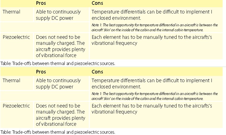
Conclusion With respect to the energy source choice, there are tradeoffs between thermal and piezoelectric sources. The table summarizes the pros and cons between these two methods. With analog switchmode power supply design expertise in short supply around the globe, it has been difficult to design an effective energy harvesting system as illustrated in figure 1. However, the LTC3108 and LTC3588-1 are touted to extract energy from almost any source of heat or mechanical vibration, both of which are commonly found in an airplane environment.

Figure 2: The LTC3108 used in a wireless remote sensor application powered from a TEG (Peltier cell).


